
The AI chip gold rush is over. What’s replaced it is something far more interesting: an era of radical specialization where the silicon itself is becoming as bespoke as the models running on it.
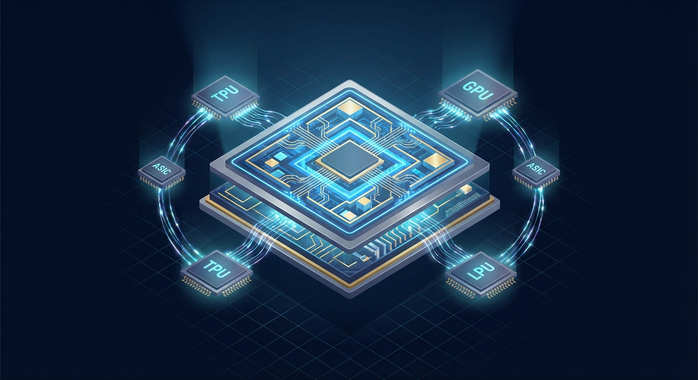
If you’ve been paying attention to the semiconductor industry over the past few years, you’ve watched a fascinating transformation unfold. The frantic scramble for any available GPU that characterized 2023–2025 has given way to something more deliberate—a strategic divergence between general-purpose graphics processors and an expanding universe of custom accelerators. TPUs, ASICs, LPUs—these aren’t just acronyms anymore. They represent fundamentally different philosophies about how to build the physical infrastructure of intelligence.
In this post, I’ll break down where the AI chip landscape stands as of April 2026, why the hyperscalers are increasingly designing their own silicon, and what this means for the future of AI infrastructure.
The End of the GPU Monoculture
For the better part of a decade, NVIDIA’s CUDA ecosystem created a de facto monoculture in AI compute. If you wanted to train a neural network, you bought NVIDIA GPUs. The software stack was mature, the developer tooling was unmatched, and the alternatives were—charitably—underbaked.
That’s changing. Not because NVIDIA stumbled, but because the economics of scale have shifted. When you’re spending billions annually on compute, the “NVIDIA tax”—the premium paid for general-purpose flexibility—starts looking like an unsustainable operational burden.
The numbers tell the story. Anthropic’s annualized revenue jumped from $9 billion at the end of 2025 to over $30 billion by early 2026. At that scale, the cost difference between renting merchant silicon and designing purpose-built accelerators becomes measured in billions of dollars annually. The math simply demands vertical integration.
This isn’t theoretical. Anthropic recently finalized a “triangular” partnership with Google and Broadcom securing approximately 3.5 gigawatts of next-generation TPU-based compute capacity starting in 2027—roughly triple their 2026 consumption levels. They’re also exploring designing their own chips, following the trajectory blazed by Meta and OpenAI.
Broadcom: The Silent Architect
If NVIDIA is the public face of the AI chip revolution, Broadcom is its hidden backbone. The company has become the indispensable gatekeeper of custom silicon, with a market cap now exceeding $1 trillion.
Broadcom’s success lies in its “full-stack” intellectual property portfolio. They’re not competing with NVIDIA on merchant silicon—they’re enabling everyone else to do so. Their client list reads like a who’s-who of AI infrastructure: Google’s TPU v7 “Ironwood,” Meta’s MTIA accelerator, ByteDance’s AI processor, and OpenAI’s forthcoming custom chip are all built on Broadcom IP.
The technical capabilities are staggering. Broadcom’s latest designs feature 9.6 Tbps SerDes interconnects on 3nm process technology, with 2nm roadmaps already in place for 2027. Their revenue from AI-specific sales is projected to exceed $25 billion in fiscal year 2026.
What makes Broadcom’s position particularly interesting is how they’ve decoupled their success from the volatile commodity chip market. They’re not betting on any single architecture winning—they’re betting on the fact that everyone will need custom silicon, and they’ll provide the building blocks.
NVIDIA’s Counter-Move: The Vera Rubin Platform
Don’t count NVIDIA out. They’ve responded to the custom silicon wave not by fighting it, but by absorbing it.
The Vera Rubin platform, which entered full production in Q1 2026, represents NVIDIA’s transformation from chip manufacturer to “AI infrastructure and factory operator.” The headline specs are impressive: 336 billion transistors on TSMC’s 3nm process, 288GB of HBM4 memory with 22 TB/s bandwidth, and 50 PFLOPS of FP4 inference performance.
But the more interesting move was their $20 billion acquisition of Groq. Remember Groq’s Language Processing Units and their deterministic scheduling architecture? NVIDIA didn’t try to replicate it—they bought it and integrated it.
The current data center configuration runs Vera Rubin GPUs for the “prefill” stage of inference (processing input context) while Groq LPUs handle the “decode” stage (generating output tokens). This hybrid approach delivers a claimed 10x reduction in inference costs compared to the previous Blackwell generation.
NVIDIA is essentially saying: “You can build your own chips, or you can buy our integrated stack that does everything.” For most organizations, the latter remains far more practical.
The Hyperscaler Arsenal
The four largest cloud providers have now all deployed second- and third-generation custom silicon. This isn’t experimentation anymore—it’s standard operating procedure.
Microsoft’s Maia 200 launched in early 2026, built on TSMC’s 3nm process with 216GB of HBM3e. Microsoft positions it as an inference workhorse for GPT-5.2, claiming 30% better performance-per-dollar than rented NVIDIA hardware.
Google’s TPU v7 “Ironwood” is the first custom ASIC to reach seven-figure deployment volume at a single customer—that customer being Anthropic. Built on N3E process, it delivers 4,614 teraFLOPS of peak FP8 compute. Google assembles these into pods of 9,216 accelerators interconnected via proprietary optical mesh fabric.
AWS’s Trainium 3 continues Amazon’s aggressive silicon roadmap, optimized for high-throughput pre-training workloads. Trainium 4 has already been announced.
The collective market shift these chips represent? Approximately $604 billion.
The Challengers: Wafer-Scale and Beyond
While hyperscalers focus on cost-efficient inference at scale, a new class of specialized hardware is pushing the fundamental limits of what’s physically possible.
Cerebras Systems is preparing for a landmark IPO in Q2 2026 with an estimated valuation exceeding $23 billion. Their Wafer-Scale Engine 3 remains the world’s largest single processor: 4 trillion transistors, 900,000 AI-optimized cores. The architecture provides 7,000 times the memory bandwidth of HBM3e systems by keeping entire AI models on-chip.
The performance claims are aggressive but apparently substantiated: Cerebras demonstrated running Llama-4 models up to 21 times faster than equivalent NVIDIA clusters. OpenAI has signed a contract for 750 megawatts of Cerebras compute.
Tenstorrent, led by legendary chip architect Jim Keller, has captured roughly 12% of the emerging RISC-V-based AI accelerator segment. Their strategy focuses on modular processor designs and avoiding ARM licensing constraints. At CES 2026, they unveiled a compact AI accelerator device with Razer that allows developers to run LLMs locally via Thunderbolt 5.
Intel acquired SambaNova Systems for $1.6 billion to bolster their Gaudi 4 roadmap, aiming to provide a credible alternative to the NVIDIA/Broadcom duopoly.
The Manufacturing Bottleneck Has Moved
Here’s something that gets less attention than it should: the “front line” of the AI revolution has moved from the transistor to the package.
TSMC has successfully scaled its CoWoS (Chip-on-Wafer-on-Substrate) capacity from 35,000 wafers per month in 2024 to a projected 130,000 by the end of 2026. This expansion is driven by the pivot from CoWoS-S to CoWoS-L, which uses local silicon interconnects to “stitch” multiple chiplets together.
This packaging technology is essential for chips like Rubin, which exceed the “reticle limit” of traditional lithography—meaning they’re physically too large to manufacture on a single exposure. TSMC has repurposed entire facilities, including the massive AP8 plant in Tainan, to handle the intricate vertical stacking these 2026-class accelerators require.
The HBM market has similarly undergone a “phased” mass production shift to HBM4, with Samsung and SK Hynix locked in fierce competition. Samsung’s 12-layer HBM4 achieves speeds of 11.7 gigabits per second. Micron has doubled its market share to 21% by aggressively capturing demand during Samsung’s earlier qualification delays.
The CUDA Moat Is Leaking
Perhaps the most significant long-term trend: NVIDIA’s proprietary CUDA software ecosystem—the real barrier to entry for competitors—is finally facing credible alternatives.
OpenAI’s Triton compiler has emerged as the industry standard for hardware-neutral development. Triton allows research teams to run models on AMD, Intel, and custom ASICs without rewriting their codebase. This matters enormously for the next generation of multimodal robotics and agentic AI, which requires switching between different accelerators based on real-time efficiency requirements.
AMD’s MI455X and Intel’s Gaudi 4 have captured significant market share in the inference layer specifically because CUDA’s lock-in is weakest there.
NVIDIA’s response has been strategic: they’ve committed $26 billion over five years to develop open-weight AI models optimized for their Vera Rubin platform. The play is to deepen developer loyalty through content rather than platform lock-in.
The Agentic AI Hardware Rebalancing
The transition from user-initiated generative AI to autonomous agentic systems is quietly reshaping hardware requirements in unexpected ways.
In agentic workflows—where AI systems pursue long-term goals involving tool invocation, logic gating, and persistent memory management—the bottleneck has shifted from GPU-centric inference to CPU-heavy orchestration. CPUs handle control flow management, coordination between multiple agents, and interaction with external APIs and vector stores.
Experimental benchmarks show that in agentic pipelines, CPU operations often dominate total runtime. In financial anomaly detection workflows, for instance, document retrieval and enrichment tasks (CPU-bound) consume significantly more time than GPU-based model inference.
Infrastructure sizing recommendations have accordingly shifted. The recommended CPU-to-GPU ratio has moved from 8:1 in 2024 to between 1:1 and 1.4:1 in 2026. Under-provisioned CPU resources cause expensive GPUs to sit idle.
Even Apple has entered the AI server market with “Project ACDC” (Apple Chips in Data Center), developing specialized “Baltra” chips for their Private Cloud Compute environment. By 2027, they plan to operate entire data centers in Houston filled with American-made servers.
China’s Parallel Universe
The AI chip market has bifurcated along geopolitical lines. U.S. export restrictions have effectively created a self-sufficient Chinese semiconductor ecosystem, with domestic chips capturing 35% of the local server market.
Huawei’s Ascend series is the primary beneficiary of NVIDIA’s reduced China presence. Huawei plans to nearly double production of its Ascend 910C to 600,000 units in 2026, targeting 50% domestic market share. The Ascend 950, 960, and 970 are scheduled through 2028.
These chips still significantly lag Vera Rubin in raw performance—the Ascend 950 provides only about 6% of the VR200’s capability—but they’ve achieved tangible market traction through government mandates and domestic software stack development.
Shanghai Biren Technology made its Hong Kong Stock Exchange debut in January 2026. Moore Threads launched the MTT S5000 GPU and the “MTT AI Book,” a laptop powered by an in-house ARM-based CPU with 50 TOPS of AI compute.
What This Means Going Forward
The AI chip landscape of 2026 is no longer defined by the singular pursuit of more FLOPs. It’s characterized by sophisticated multi-vendor strategies where specific workloads determine silicon architecture.
Two trajectories have emerged:
Hyperscale Bespoke Silicon: Google, Microsoft, Amazon, and Meta have successfully decoupled their infrastructure from the general-purpose GPU market, using custom ASICs to drive down inference costs and improve power efficiency.
High-End Factory Platforms: NVIDIA has maintained dominance by transforming into an infrastructure operator, integrating deterministic scheduling and massive memory bandwidth to handle the most complex agentic and multi-modal workloads.
Anthropic’s $50 billion infrastructure investment and their triangular deal with Broadcom and Google signal that the future of AI will be built on full-stack vertical integration. As the industry moves toward 2nm nodes and wide-scale adoption of co-packaged optics, competitive advantage will belong to those who master the entire physical fabric—from transistors to optical interconnects to the compilers that bind them together.
The silicon hegemony of the past is being replaced by a diverse, specialized, and highly resilient architecture of autonomy. The question isn’t whether you use NVIDIA or something else. It’s whether your compute infrastructure matches your actual workload—and whether your organization has the sophistication to make that determination.
The semiconductor industry moves fast. If you found this analysis useful, subscribe for more deep dives into the infrastructure powering the AI era.